A team of researchers led by Dr. Deep Jariwala, assistant professor of Electrical and Systems Engineering at Penn’s School of Engineering and Applied Science, recently invented a cutting-edge design and method to create superlattices (alternating stacks of two-dimensional materials) and semiconductors to obtain strong light absorption for next-generation optical devices.
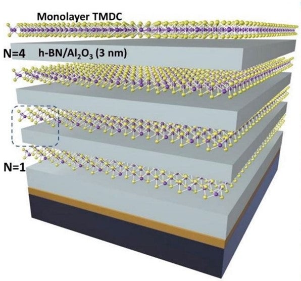
Next-generation optical technologies like light detection and ranging (LiDAR) and on-chip optical modulators have been applied to self-driving vehicles, device communication, and computing. Existing technologies often use transition metal dichalcogenides (TMDs), which have highly desirable optical and electronic properties, but offer uneven sample thickness, small lateral dimensions, and weak light absorption.
Dr. Jariwala and his team have addressed this problem by developing superlattices that offer controllable thickness, device-scale lateral size, and strong light absorption. In addition, they maintain the quantum effects found in TMD monolayers, which introduces new and improved avenues for optical device engineering.
PCI is actively seeking potential partners and investors for further development of this exciting technology opportunity. You can find more information about the technology here.